
 admin
adminWhat is SMT Assembly?
Surface Mount Technology (SMT) Assembly is a critical process in the manufacturing of modern electronic devices. It involves mounting electronic components directly onto the surface of pcb smt assembly (PCBs). This technology has largely replaced the older through-hole technology, offering numerous advantages in terms of size, performance, and automation. Here’s a comprehensive guide to understanding SMT Assembly:
SMT Assembly refers to the method of constructing electronic circuits where the components are placed directly onto the surface of PCBs. These components, known as Surface Mount Devices (SMDs), are designed to have small terminals or leads that can be soldered onto the PCB pads. These active components are also available in surface-mount packages, providing enhanced performance and reduced space requirements.
PCBs in SMT have specially designed pads and tracks to accommodate SMDs. These pads are coated with a layer of solder paste to facilitate the soldering process. SMT allows for multi-layer PCBs, which can support more complex and compact circuit designs. The SMT assembly process involves several steps to ensure the precise and efficient placement of components:
The process begins with the application of solder paste to the PCB. This is done using a stencil that matches the PCB layout, ensuring that solder paste is deposited only on the pads where components will be placed. The stencil ensures accuracy and consistency, which are crucial for high-quality assembly.
After applying the solder paste, SMDs are placed onto the PCB. This step is usually performed by high-speed pick-and-place machines that can accurately position components based on programmed coordinates. These machines can handle thousands of components per hour, significantly speeding up the assembly process.
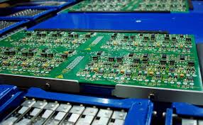
What is SMT Assembly?: A Must-read Guide
Once all components are placed, the PCB undergoes reflow soldering. In this step, the board is passed through a reflow oven where it is gradually heated. The solder paste melts and forms a solid bond between the components and the PCB pads. The controlled temperature profile in the oven ensures that the components and solder joints are not damaged.
Post-soldering, the assembled PCBs are inspected for defects. This can be done using Automated Optical Inspection (AOI) systems that use cameras to check for missing components, solder bridges, and other defects. X-ray inspection is also used, especially for checking hidden solder joints in complex components like BGAs.
SMT allows for smaller component sizes and more compact circuit designs. This is essential for modern electronic devices that demand high functionality in smaller form factors, such as smartphones and wearable devices.
While the initial setup costs for SMT assembly can be high due to the need for specialized equipment, the overall production costs are reduced due to faster assembly times, fewer defects, and the ability to handle large production volumes efficiently.
SMT Assembly is a cornerstone of modern electronics manufacturing, enabling the production of compact, high-performance, and cost-effective electronic devices. Understanding the SMT process, from solder paste application to inspection, highlights its advantages and the reasons for its widespread adoption in the industry. Despite its challenges, the benefits of miniaturization, high-speed production, and enhanced performance make SMT Assembly an essential technology in the electronics sector.