
 admin
adminflexible PCB fabrication differ from rigid PCBs
Printed circuit boards (PCBs) are essential to many modern products. They’re the substrate on which circuits are laid and act as a foundation for the component mounting, wire routing and shielding. PCBs are used in everything from smartphones and tablets to robots and aircraft. However, traditional rigid PCBs aren’t always ideal for every application. For those that require added flexibility, the flex PCB fabrication process offers an alternative. Flex PCBs are created using specialized materials and construction techniques. But how does the flex PCB manufacturing process differ from standard rigid PCBs?
Flex PCBs are designed to fit into a tight space and feature flexible conductor paths that can withstand the stress of repeated bending. This is accomplished through the use of specialized flex dielectrics and ultra-thin copper foils. This allows for a much smaller overall size than standard PCBs. It’s also possible to create multilayer flex PCBs, with some layers being flexible and others being rigid.
Like standard PCBs, the flexible pcb fabrication process requires an effective design to ensure a successful end-product. The design should be optimized for production and adhere to stricter dimensional specifications. This will help to avoid the possibility of a failure caused by excessive expansion or contraction of the flex PCB.
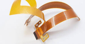
How does flexible PCB fabrication differ from rigid PCBs?
Once the design has been optimized, it’s time to get started with the flex PCB fabrication process. The first step is to prepare the flex PCB by applying an epoxy resin, or adhesive, onto the surface. Then, the flex PCB is laminated onto a base substrate. Polyimide is the most common flex substrate material given its high durability, thermal properties and cost-benefit ratio. The conductive paths or traces are then formed on the flex circuit by patterning the copper with lithographic processes. Typically, the conductive paths are on both sides of the flex circuit.
The flex PCB is then protected by an optional coverlay layer, which also acts as the solder mask. The most common coverlay is additional polyimide film with an adhesive, though there are also adhesive-less processes available. If there are components mounted on the flex circuit, it’s important that those areas be covered with a photo-imageable solder mask.
After the coverlay has been applied, it’s time to apply stiffeners if needed. These are placed on one or both sides of the flex circuit to prevent warpage during soldering or bending. Stiffeners can be either spring-loaded or not depending on the flex circuit’s application. For example, a stiffener on one side of the board can be spring-loaded to provide structural support for high-speed inserts.
It’s common for robust flex PCBs to withstand millions of dynamic bend cycles in consumer grade applications. The key is to properly design the flex circuit by taking into account aspects like trace spacing, minimum bend radius, adhesives, and tear propagation resistance. Careful design can enable a flex circuit to deliver the performance required in today’s portable electronic devices.