
 admin
adminRF PCBs Handle High-Frequency RF Signals
High-frequency RF signals are crucial to a wide range of modern applications. The specialized engineering and meticulous attention to detail required for designing pcba circuit board that handle these signals is essential in ensuring the quality, reliability, and performance of the final product. The design process for RF PCBs involves careful consideration of a variety of factors, including impedance matching and electromagnetic interference (EMI). Any deviations from the ideal design can lead to signal loss or distortion, impacting system performance. In addition, proper routing and isolation are critical to avoiding crosstalk-induced signal distortions.
Impedance matching is essential for ensuring efficient power transfer and minimizing signal reflections. In RF PCBs, impedance matching is accomplished through the use of transmission lines. These transmission lines are comprised of two conductors with a specific characteristic impedance surrounded by a dielectric material. This configuration allows signals to travel long distances without experiencing significant loss or degradation. The characteristic impedance of transmission lines is determined by factors such as their width, spacing, and the dielectric properties of the underlying substrate.
RF PCBs require special materials with a low dielectric constant and dispersion to minimize losses and maintain their electrical characteristics over a wide frequency spectrum. Conventional FR4 substrates can be suitable for lower-frequency applications, but the superior electrical properties of Rogers materials, Teflon, and ceramic substrates are typically preferred in RF circuit boards. These materials have a much lower Coefficient of Thermal Expansion than FR4, and they also provide greater electrical stability and improved performance at higher frequencies.
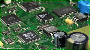
How Do RF PCBs Handle High-Frequency RF Signals?
The physical layout and component placement on a RF PCB are critical to its performance. It is essential to minimize the length of the traces, as long traces are more susceptible to losses and distortions. RF traces must be kept as short as possible to minimize attenuation and ensure that the traces do not interact with each other, a condition known as crosstalk. Using differential signaling and ground planes can help to eliminate crosstalk and improve isolation between traces.
In addition, RF traces should be spaced apart as far as possible to prevent the accumulation of capacitance that can cause a loss in signal integrity. It is also important to avoid the use of vias, as they can introduce parasitic capacitance that may interfere with signal transmission.
The RF PCB manufacturing process begins with the preparation of a prototype, which is then etched and soldered to assemble the circuit board. During the fabrication stage, the prototype undergoes inspection techniques such as Automated Optical Inspection (AOI) and X-ray to detect any defects that could compromise the board’s functionality or performance. Finally, the RF PCB is tested with time-domain reflectometry and network analysis to determine if it performs as designed. The resulting data can be used to make any necessary modifications and produce a final RF PCB that meets all performance criteria. This iterative testing process ensures that the RF circuit board is optimized for performance and reliability. This is essential in enabling the seamless wireless communication and advanced radar and sensing systems that drive technological advancements across industries.