
 admin
adminPCB assembly differ from PCB fabrication
In the realm of electronics manufacturing, two critical processes stand out: PCB assembly and PCB fabrication. While they are interconnected and essential for creating functional electronic devices, they serve distinct purposes and involve different stages. Understanding the differences between pcb assembly and PCB fabrication is crucial for grasping their roles in the production of printed circuit boards (PCBs).
PCB fabrication, also known as PCB manufacturing or PCB production, is the initial stage in the creation of a printed circuit board. This process involves the manufacturing of the bare PCB itself, which serves as the foundation for the electronic components to be assembled upon. PCB fabrication begins with the design of the PCB layout, specifying the arrangement of traces, pads, and other features on the board.
The fabrication process typically starts with the preparation of the substrate material, which is commonly made of fiberglass-reinforced epoxy resin known as FR-4. The substrate is then coated with a layer of copper on both sides, forming the conductive pathways (traces) that will carry electrical signals between components. A photosensitive film is applied to the copper layer, and the PCB layout design is transferred onto it using a process called photolithography.
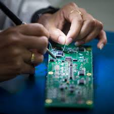
How does PCB assembly differ from PCB fabrication?
Once the PCB layout is transferred, the excess copper is etched away using chemical etchants, leaving behind the desired traces and features on the board. After etching, the photosensitive film is removed, and the board undergoes drilling to create holes for through-hole components and vias, which provide electrical connections between different layers of the PCB.
PCB fabrication concludes with the application of surface finish and solder mask to protect the exposed copper traces and facilitate soldering during PCB assembly. Surface finishes such as HASL (Hot Air Solder Leveling), ENIG (Electroless Nickel Immersion Gold), and OSP (Organic Solderability Preservatives) are applied to prevent oxidation and ensure solderability.
In contrast, PCB assembly refers to the process of populating the bare PCB with electronic components to create a functional circuit. This process follows PCB fabrication and involves mounting and soldering various components onto the fabricated PCB. PCB assembly encompasses several stages, including solder paste application, component placement, soldering, inspection, and testing.
Solder paste, a mixture of tiny solder particles and flux, is applied to the surface of the bare PCB using a stencil during PCB assembly. This paste acts as an adhesive to hold the components in place during the soldering process. Automated pick-and-place machines then accurately place the electronic components onto their designated positions on the PCB.
Once all components are placed, the PCB undergoes soldering to create secure electrical connections between the components and the PCB. Soldering techniques such as reflow soldering, wave soldering, or hand soldering are employed, depending on the type of components and production requirements.
After soldering, the assembled PCB undergoes inspection to detect any defects or inconsistencies. Automated optical inspection (AOI) systems are commonly used to scan the board for issues such as missing components, misalignment, or soldering defects. Functional testing may also be performed to verify the functionality and performance of the assembled PCB.
In conclusion, while PCB fabrication and PCB assembly are interconnected processes essential for creating printed circuit boards, they serve distinct purposes and involve different stages. PCB fabrication focuses on manufacturing the bare PCB, while PCB assembly involves populating the fabricated PCB with electronic components to create functional electronic devices. Understanding the differences between these two processes is vital for comprehending the intricacies of electronics manufacturing and ensuring the successful production of high-quality PCB assemblies.